International Journal of Theoretical and Applied Nanotechnology (IJTAN)
ISSN: 1929-1248

Volume 1, Issue 2, Year 2013 - Pages 30-40
DOI: 10.11159/ijtan.2013.004
On Contact Resistance of Carbon Nanotubes
Libao An¹, Xiaoxia Yang¹, Chunrui Chang²
¹College of Mechanical Engineering, Hebei Provincial Key Laboratory of Inorganic Nonmetallic Materials, Hebei United University,
Tangshan, Hebei 063009, China
lan@heuu.edu.cn; yangxx0926@163.com
²College of Sciences, Hebei United University, Tangshan, Hebei 063009, China
changchunrui@heuu.edu.cn
Abstract - Carbon nanotubes (CNTs) have found many potential applications stemming from their small dimensions and marvellous electronic, mechanical, and thermal properties. One of the barriers for using CNTs as building blocks in nanoelectronics is the high contact resistance. This paper reviews recent progress on the research of contact resistance of CNTs. It starts with a preview of two basic contact configurations, i.e., side contact and end contact, and measurements of contact resistance. The formation of Schottky barrier on a typical metal-semiconductor contact is then presented, aiming at looking for ways to reduce contact resistance from a theoretical point of view. The current techniques for improving CNT contact resistance are classified and summarized as well. The principles and applicabilities of these techniques are compared and discussed. A deep understanding of the forming mechanisms and improvement methods of contact resistance is critical in order to bring CNT-based devices from laboratory to the real-world technology.
Keywords: Carbon nanotube, contact resistance, Schottky barrier, resistance reduction, review.
© Copyright 2013 Authors - This is an Open Access article published under the Creative Commons Attribution License terms. Unrestricted use, distribution, and reproduction in any medium are permitted, provided the original work is properly cited.
Date Received: 2013-09-19
Date Accepted: 2013-11-11
Date Published: 2013-12-30
1. Introduction
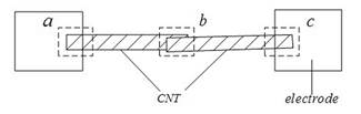
Carbon nanotubes (CNTs) have attracted intense interest during the past two decades attributed to the small dimensions and particular properties in electronic, mechanical, thermal, optical and other aspects as previously shown [1-8]. These characteristics make CNTs promising materials for a wide variety of applications such as field emission displays, energy storage, interconnects, sensors and probes [9-16]. The contact resistance of CNTs indicates the electrical resistance arising from the interface between a CNT and a metal contact when a CNT is connecting with a pair of electrodes. It also means the resistance of a CNT-CNT junction when an overlapped joint takes place between two CNTs. The two cases are demonstrated in Fig.1, in which the CNT-CNT contact is shown in the middle dashed box b, and the CNT-metal contacts are shown in the other two boxes a and c, as explained by Ranjan and Mertig [17]. The contact resistance plays a key role in the application of CNTs in nanoelectronics. Therefore, a deep understanding of the electrical properties of the contacts is essential for bring CNT-based devices from laboratory to the real-world technology.
The geometries of the CNT contacts with metals are commonly divided into two classes: side contacts and end-bonded contacts. For side contacts, which are often produced when CNTs are simply placed on the surface of metal electrodes, the bonding is produced by the van der Waals force. This weak force not only attracts CNTs to deposit on the electrodes, but also brings an effective insulating layer which contributes much to the contact resistance as descried in [18, 19]. For end contacts, Zhang et al. [20] descried that the bonding between CNT and metal is atomic, and these contacts are often formed by reacting CNTs with metals.
2. Measurement of Contact Resistance
2. 1. Contact Resistance of Individual CNTs
Four-probe electric measurements of contact resistance of multi-walled carbon nanotube (MWNT)-metal have been completed by Bachtold et al. [21]. The values of contact resistance were in the range of 1 MΩ-1 GΩ. Lee et al. [22] distinctly found that the contact resistance was normally greater than 10 MΩ before any treatment. Martel et al. [23] obtained the saturation value of electric current flowing through field effect transistors (FETs) based on individual single-walled carbon nanotubes (SWNTs) and MWNTs. The contact resistance which corresponded to the current was about 1.1 MΩ. Two-probe and four-probe measurements between SWNT and Pt electrode showed high contact resistance between 1-4 MΩ at 300 K as revealed by Bezryadin et al. [24]. Kong et al. [25] performed ab initio pseudopotential calculation for a nanocontact between SWNT and copper electrode. They explained why a huge contact resistance of the order of 1 MΩ being there theoretically. The way up to date of measuring and calculating contact resistance with the help of focused ion beam (FIB) has been recommended by An et al. [26]. The contact resistance of MWNT with Au was around 100 kΩ/μm and that between two MWNTs could be as low as 50 kΩ.
Table 1. Values of measured contact resistance
|
Contact type |
Values of contact resistance |
References |
|
Between metal and CNT |
1 MΩ-1 GΩ (Metal-MWNT) |
[21] |
|
>10 MΩ (Au/Ti-CNT) |
[22] |
|
|
~1.1 MΩ (Au-SWNT) |
[23] |
|
|
1-4 MΩ (Pt-SWNT) |
[24] |
|
|
~1 MΩ (Cu-SWNT) |
[25] |
|
|
Between two CNTs |
>50 kΩ (MWNT-MWNT) |
[26] |
2.2. Contact Resistance of CNT Bundles
When acting as interconnects, CNTs have the same functions as the traditional cooper material and produce a lower resistance in parallel connections than in serial connections, particularly in the case of CNT bundles. At present, several researchers have fabricated vertical CNT bundles and committed to their integration into devices [4, 27-30]. A four-terminal Kelvin structure was applied to measure the current-voltage characteristics of the CNT via interconnects and the whole resistance was 92 kΩ as shown by Katagiri et al. [27]. The study has also attested that the contact resistance is higher than the CNT conducting resistance in the whole CNT path through measurement and calculation. Chiodarelli et al. [28] grew CNTs on a nickel film into the contact holes at 400 °C and then the holes were filled with SiO2. The length of the tubes and the contacts were controlled by chemical mechanical polish (CMP), and CMP could also develop a flat surface which increases the number of CNTs in contact with the top Au/Ti electrode. Another advantage of CMP is opening MWNT caps, which provides conduction paths of the inner shells. In their experiments, the total resistance of 576 parallel CNT bundles at 0.1V was 103.9±2.8 Ω.
From Table 1, it is known that the measured values of contact resistance varied widely among experiments. Actually, the techniques for fabricating electrodes, the quality of CNTs, and the contact configurations of CNT/metal all have effects on the contact resistance. It can also be concluded that the contact resistance is usually high. For CNT bundles, although the obtained values of contact resistance are much smaller than those for individual CNTs as shown in Table 1, there is still enormous potential in reducing their contact resistance.
3. Reasons for High Contact Resistance
3. 1. Schottky Barrier
Since the first introduction of the carbon nanotube field effect transistor (CNTFET) made by semiconducting CNTs as previously shown [31], significant research efforts have been made for understanding the mechanisms of CNTFET, such as the large current density, the high mobility, and the controlled response to the gate voltage [32-34]. Martel et al. [35] and Javey et al. [36] demonstrated the existence of the Schottky barrier and its unfavourable roles in the operation of CNTFETs. A low Schottky barrier in such CNTFETs is expected. As well, to design highly desirable CNT devices with low consumption at CNT-metal contact, reduction of contact resistance resulting from Schottky barriers is required.
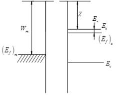
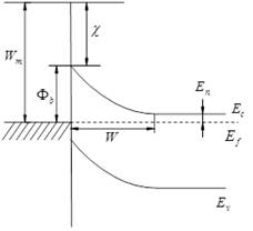
A Schottky barrier exists at a typical metal-semiconductor contact. Before metal comes into contact with semiconductor (N-type for example), their energy band structures are represented in Fig. 2. If the workfunction of the metal (Wm) is greater than that of the semiconductor (Ws=χ+En), the electrons in the semiconductor would move towards the metal once the two materials are joined, forming a positive space charge region (depletion region) on the surface of the semiconductor. In this region, the formed electrostatic field, pointing from the semiconductor to the metal, prevents further flowing of the electrons until the whole system reaches an equilibrium state. During this process, the Fermi level of the metal is moving up and that of the semiconductor is going down until they are on the same level, forming the Schottky barrier as shown in Fig.3. The Schottky barrier height Фb is given by:
|
Фb=Wm–χ. |
(1) |
The emergence of Schottky barriers at the interface is detrimental to charge injection and leads to large contact resistance. Electrons must overcome the barrier to flow through the contact, and the main transport mechanisms are thermionic emission and tunnelling. The latter will dominate when the depletion regionis thin enough [37].The width of the depletion region W is given by
|
W=R exp (2ε0Фb/ρNAR), |
(2) |
where R denotes the nanotube radius, ρ is the number of dopants per carbon atom and NA is the number of carbon atoms per unit area [38]. Therefore, an effective way to reduce W for tunnelling is semiconductor doping.
3. 2. Other Influencing Factors
The contact area largely determines the size of the contact resistance between CNTs and metal electrodes [39]. The dependence of the contact resistance on the contact length for side-contacts has been experimentally [40, 41] and theoretically [42, 43] explained. The workfunction and wettability of the metal electrode can also influence the magnitude of the contact resistance [44-46]. If a stronger cohesion takes place at the carbon-electrode interface, a thinner vacuum gap could be obtained [30, 47]. The contact resistance would go down when the number of conducting shells in MWNTs increases [28, 48]. In addition, the local chemical contamination around the contact produces some oxides which act as a tunnel barrier, and the tunnel barrier would be a part of the contact resistance [49].
4. Reduction of Contact Resistance
4. 1. Thermal Annealing
Lee et al. [22] put forward a relatively simple and reliable method of rapid thermal annealing (RTA) to reduce the contact resistance of CNTs with Au/Ti electrodes. Before the RTA, the contact resistance was normally greater than 10 MΩ. After the RTA at 600-800 °C for 30 s under vacuum, it considerably decreased by several orders of magnitude with the values of 0.5-50 kΩ. And after three months, the good and long-term stable contacts were still constant between CNTs and electrodes. It was also reported that the result was attributed to the formation of Ti-carbides at the end contacts by Zhang et al. [20]. Another possible reason is the gradual increase of contact area during the annealing process [22]. Some other experiments [50-53] built on thermal annealing have also achieved satisfactory contact resistances.
For CNT bundles, as described in [28], the thermal annealing at 400°C for 30 minutes improved the contact between CNT bundles and Ti layer, and the whole resistance of 576 parallel CNT bundles decreased to 40.7±0.7 Ω after annealing. Katagiri et al. [27] applied dilute hydrofluoric (HF) acid treatment after CMP, and the whole resistance of planarized CNT via interconnects with 160-nm-diameter was reduced to 3.8 kΩ. Then the thermal annealing was performed at 450°C and the resistance decreased further to 1.5 kΩ. Again, the formation of TiC at the contacts was an explanation.
4. 2. Electric Current Flowing
There have been a few studies making use of direct current (DC) flow through the electrodes to adjust the contact with CNTs [54, 55]. As previously shown in [55], the contact resistance was lowered from 0.57-39 MΩ to 15-50 kΩ after a DC current flowing through Au/Ti electrodes for a certain period of time, which was attributed to the formation of TiC once more. Asaka et al. [56] presented a method in which a current with a density of 108 A/cm2 flowed through the CNT-metal junction. The surface of Au electrodes began to melt due to the Joule heating which made the contact area larger for reducing the contact resistance. However, if the DC current flows through continuously, the device could be entirely destroyed by dissolving the metal.
To avoid the failing, one shot of electrical pulse instead of DC current was applied on a side contact which was made of an individual SWNT and Pd electrode [57]. By only heating the contact temporarily and transferring little quantity of heat to the substrate, the contact resistance could decrease from 324 kΩ initially to 66 kΩ after the pulse annealing. Nurbawono et al. [58] also showed an effective way by applying a controllable pulse current to flow through the electrodes. It was said that the method could reduce the height of Schottky barriers at metal-CNT interfaces, resulting in improved conductivity of CNT-based FETs.
Chen et al.[59] developed a novel batch welding of aligned CNTs onto electrodes by radio frequency induction heating in vacuum. After the induction heating process, the measured resistance values by two-terminal method were in the range of 15-30 kΩ, a considerable decrease compared to the initial range of 1-3 MΩ before the treatment. The amazing result comes from the heat offered by eddy current, and the surface of the CNTs in the contact area could be covered by the molten metal.
4. 3. Electron Beam Irradiation
Bachtold et al. [21] used electron beam exposed to the contact area in a scanning electron microscope (SEM), enhancing the transmission of electrons between Au and CNT. When the total dose of beam achieved 0.7 C/cm2 and the exposure time was an hour or more, the two-terminal resistance dropped considerably to 30 kΩ from an original value greater than 100 MΩ. Ando et al.> [60] also obtained good CNT/Pt contacts by selective electron beam irradiation under DC-biased condition in field emission (FE)-SEM chamber. The current was very low before treatment, but it increased dramatically to -20 μA by the irradiation at -5 V. The contact resistance was reduced to less than 250 kΩ in the end.
The approaches stated above are all effective in reducing contact resistance. Not only the generation of carbides, but the evaporation of water and residual solvents as well as the decomposition of attachments at the junction could also improve the status of the contact. The melt of metal electrode caused by high temperature would bring a larger contact area. However, the high temperature simultaneously produces some side effects such as the destruction of electrodes and the structural change of CNTs.
4. 4. Ultrasonic Bonding Technique
Chen et al. [61, 62] put forward an ultrasonic bonding technique for bonding SWNTs onto Ti microelectrodes to create low-resistance and reliable contacts. After the sample was fixed, a clean ultrasonic bonding head was used to transfer ultrasonic energy to the interface with a duration of 0.2 s per bonding. SWNTs were pressed into or welded onto the electrodes. Using this technique, two-terminal resistances of the device were in the range of 8-24 kΩ/μm at room temperature.>
4. 5. Metal Deposition
An et al. [26] calculated the values of contact resistance of MWNT-Au and MWNT-MWNT with the help of FIB. In their experiments, tungsten thin film was deposited by FIB to cover the contact area of assembled CNTs and electrodes to make metallic contact. The precursor gas W(CO)6 was sprayed and absorbed on the sample surface and incident ion beam decomposed the gas. Then, the volatile reaction product desorbed from the sample surface, while W remained on the surface as a thin film. In their research, the contact resistance of MWNT-Au was around 100 kΩ/μm and that between two MWNTs was as low as 50 kΩ, as stated previously.
Madsen et al. [63] applied electron beam to decompose the organometallic vapor in SEM for depositing Au on the contact. After the metal deposition, the whole resistance including the conductive resistance of MWNTs and contact resistance was on the order of 100 Ω. Vilà et al. [64] obtained metallic contacts to access different nanometer-sized materials using a dual-beam FIB instrument which was equipped with a C9H16Pt injector to deposit Pt. Ranjan and Merrtig [17] reported the improvement of contact resistance of CNTs by the deposition of metal from an aqueous Pd salt solution. The overall resistance was below 1 MΩ in their experiments.
4. 6. Hydrocarbon Molecule Deposition
It has been reported that CNTs and hydrocarbon are made of the same kind of element and a low-resistance contact could be achieved by taking advantage of hydrocarbon to link CNTs to electrodes [65]. A piezodriven nanomanipulator inside a transmission electron microscope (TEM) was used to make an electrical contact between two MWNTs. In the study, two MWNTs were first glued onto the piezodriven probe and the ground electrode respectively. The piezodriven probe was adjusted in all three dimensions, making the tips of the two MWNTs close enough to each other. Then the electrostatic attraction could make the CNTs a tip-to-tip contact. The TEM chamber was full of hydrocarbon gas. Under electron beam irradiation, the hydrocarbon molecules were polarized and attracted by the charged nanotubes due to the applied voltage, and aggregation of the hydrocarbon molecules took place. Finally, a hydrocarbon coating was formed on the junction, and the average contact resistance between CNTs was about 550 kΩ.
4. 7. Carbon Molecule Deposition
Actually, graphitic carbon which has same kind element and similar chemical bonding as CNT can make a better contact than hydrocarbon. Chai et al. [44] made electrical contact at the CNT-metal interface using a graphitic carbon layer catalyzed by Ni layer, and the contact status was ameliorated after annealing at 850°C in Ar or H2 ambient. The reduction of the contact resistance was ascribed to the improved wetting and formation of chemical bonding to CNTs. Meanwhile, the covalent chemical bonding between graphitic interfacial layer and CNTs can enlarge the actual contact area between the metal and CNTs. Some other researchers have also used electron beam to induce deposition of carbon for making an electrical contact inside a SEM or TEM [66, 67].
4. 8. Modest Pressure
Modest mechanical pressure could dramatically enhance the
transport of electrons between CNTs. Park et al. [68] carried
out first-principle density-functional calculations to investigate the
electronic structure of Au/CNT contact. It was found that
the pressure on
the contact can change the Fermi level and cause N-type behaviour of electronic
transport. Also, Buldum and Lu [69] reported that the contact resistance was dependent on
the charity of CNTs, the angle (![]() ) which is between two CNT axes, and the force applied on the
contact. For a
(18, 0) - (10, 10) contact between two crossing SWNTs, when the tubes were in-registry(
) which is between two CNT axes, and the force applied on the
contact. For a
(18, 0) - (10, 10) contact between two crossing SWNTs, when the tubes were in-registry(![]() =30°, 90°, 150°), the contact resistance could be decreased to 121 kΩ with mechanical pressure. The research by Allaoui et al. [70] revealed that with the increase of the compression force, the contact resistance of CNT tangles decreased and the total resistance could reach the values in the order of 100 kΩ.
=30°, 90°, 150°), the contact resistance could be decreased to 121 kΩ with mechanical pressure. The research by Allaoui et al. [70] revealed that with the increase of the compression force, the contact resistance of CNT tangles decreased and the total resistance could reach the values in the order of 100 kΩ.
4. 9. Elimination of Surface Contamination
The CMP process has always been introduced into the process of making CNT bundles for interconnect purpose, but the emergence of residual oxide layer during the CMP process makes poor electrical contact between the CNTs and metal. Lee and Lee [29] adopted two post-CMP treatments to remove residual oxide layer: one was dipping samples into diluted HF solution and the other was Ar plasma treatment. Combined with thermal annealing afterwards at 500 °C in N2 atmosphere for 10 min, the lowest whole resistance was 85 Ω.
4. 10. Doping
Based upon Formula (2), it can be perceived that the width of the depletion region W is extremely sensitive to the doping level and increases rapidly at low doping concentration as shown in Léonard et al. [37]. Johnny et al. [71] presented a novel monolayer doping (MLD) strategy for nanoscale doping of semiconductor materials. The MLD strategy was based on the formation of a highly uniform and covalently bonded monolayer of dopant-containing molecules. By RTA, the dopant phosphorus atoms could be uniformly diffused, reflecting the desired doping profile. The contact resistance of devices based on Si nanowires was significantly reduced from about 100 GΩ at 1 V to only about 2 MΩ when the Si nanowires were heavily doped using the MLD process. Some experiments have also showed that doping can enhance the conductivity of CNTs [72-75]. Similarly, the MLD process could be applied to other nanomaterials such as CNTs for reducing contact resistance.
It is now clear that it is doping in the semiconductor that reduces the width of the depletion region and thus reduces the contact resistance. Doping can finely control the physical and electrical properties of nanomaterials to overcome the Schottky barrier. Provided that the atoms in metal absorb certain energy and become active enough at the interface, some of them could more likely penetrate into semiconductive CNTs.
Various techniques for reducing contact resistance are summarizedin Table 2.
Table 2. Contact resistance reduced by various techniques.
|
Technique |
Specific operation method |
Values of contact resistance |
References |
|
Thermal annealing |
Rapid thermal annealing |
0.5-50 kΩ |
[22] |
|
Thermal annealing |
40.7±0.7 Ω |
[28] |
|
|
Thermal annealing combined with HF treatment |
1.5 kΩ |
[27] |
|
|
Electric current flowing |
DC current flow through electrodes |
15-50 kΩ |
[55] |
|
Electrical pulse flow through electrodes |
66 kΩ |
[57] |
|
|
Radio frequency induction heating |
15-30 kΩ |
[59] |
|
|
Electron beam irradiation |
Electron beam exposed to the contact area |
30 kΩ |
[21] |
|
Selective electron irradiation under DC condition |
<250 kΩ |
[60] |
|
|
Elimination of contamination |
|
85 Ω (total resistance) |
[29] |
|
Ultrasonic bonding |
Ultrasonic bonding |
8-24 kΩ/μm |
[62] |
|
Hydrocarbon deposition |
Electron beam induced deposition of hydrocarbon molecules |
≈ 550 kΩ |
[65] |
|
Carbon deposition |
Carbon molecule deposition |
|
[44] |
|
Modest pressure |
Pressure on CNT-metal contact area |
121 kΩ |
[69] |
|
Pressure on CNT tangles |
100 kΩ |
[70] |
5. Conclusions
The high contact resistance has been a major barrier for full application of CNT-based devices. There exist a variety of factors influencing the contact resistance of CNTs which include contact configuration, type of CNTs, electrode materials, fabrication process of devices, contamination status of the contact surface, among others. Doping can reduce the width of the depletion region and minimize Schottky barrier and therefore will effectively lower the contact resistance of semiconductive CNTs. Other commonly used approaches in the literature to improve the CNT contact include thermal annealing, electric current flowing, induction heating, electron beam exposure, ultrasonic bonding, and deposition of metal or inorganic materials on the contact area. The applicability of these techniques should be verified for exploring practical ways to weaken the detrimental impact of the CNT contact resistance.
Acknowledgements
The research was jointly sponsored by the National Natural Science Foundation of China (51172062), the Scientific Research Foundation for the Returned Overseas Chinese Scholars from the Ministry of Education of China, the Natural Science Foundation of Hebei Province of China (E2012209017), and the Hundred Talents Program of Hebei Province of China (E2012100005).
References
[1] A. Bachtold, P. Hadley, T. Nakanishi, C. Dekker "Logic circuits with carbon nanotube transistors" 2001, Science, 294, 1317-1320. View Article
[2] J. Bernholc, D. Brenner, M.B. Nardelli, V. Meunier, C. Roland "Mechanical and electrical properties of nanotubes" 2002, Annual Review of Materials Research, 32, 347-375. View Article
[3] J. Hone, M.C. Llaguno, M.J. Biercuk, A.T. Johnson, B. Batlogg, Z. Benes, J.E. Fischer "Thermal properties of carbon nanotubes and nanotube-based materials" 2002, Appl. Phys. A, 74, 339-343. View Article
[4] N. Chiodarelli, S. Masahito, Y. Kashiwagi, Y. Li, K. Arstila, O. Richard, D.J. Cott, M. Heyns, S. D. Gendt, G. Groeseneken, P.M. Vereecken "Measuring the electrical resistivity and contact resistance of vertical carbon nanotube bundles for application as interconnects" 2011, Nanotechnology, 22, 085302. View Article
[5] W.A. De Heer, W.S. Bacsa, A. Chatelain, T. Gerfin, R. Humphrey-Baker, L. Forro, D. Ugarte "Aligned carbon nanotube films: production and optical and electronic properties" 1995, Science, 268, 845-847. View Article
[6] A. Kis, A. Zettl "Nanomechanics of carbon nanotubes" 2008, Philosophical Transactions of the Royal Society A, 366, 1591-1611. View Article
[7] Y. Massoud, A. Nieuwoudt "Modeling and design challenges and solutions for carbon nanotube-based interconnect in future high performance integrated circuits" 2006, ACM Journal of Emerging Technologies in Computing, 2, 155-196. View Article
[8] P. Vincent, S.T. Purcell, C. Journet, V.T. Binh "Modelization of resistive heating of carbon nanotubes during field emission" 2002, Physical Review Letters, 88, 105502. View Article
[9] Z. Chen, J. Appenzeller, J. Knoch, Y.-M. Lin, Ph. Avouris "Low-frequency current fluctuations in individual semiconducting single-wall carbon nanotubes" 2005, Nano Letters, 5, 1497-1502. View Article
[10] L. Dai "Advanced syntheses and microfabrications of conjugated polymers, C60-containing polymers and carbon nanotubes for optoelectronic applications" 1999, Polymers for Advanced Technologies, 10, 357-420. View Article
[11] S. Fujii, S. Honda, H. Machida, H. Kawai, K. Ishida, M. Katayama "Efficient field emission from an individual aligned carbon nanotube bundle enhanced by edge effect" 2007, Applied Physics Letters, 90, 153108. View Article
[12] M. Terrones "Science and technology of the twenty-first century: synthesis, properties and applications of carbon nanotubes" 2003, Annual Review of Materials Research, 33, 419-501. View Article
[13] A. Naeemi, J.D. Meindl "Carbon nanotube interconnects" 2009, Annual Review of Materials Research, 39, 255-257. View Article
[14] C.V. Nguyen, Q. Ye, M. Meyyappan "Carbon nanotube tips for scanning probe microscopy: fabrication and high aspect ratio nanometrology" 2005, Measurement Science and Technology 16, 2138-2146. View Article
[15] J.A. Robinson, E.S. Snow, S.C. Badescu, T.L. Reinecke, F.K. Perkins "Role of defects in single-walled carbon nanotube chemical sensors" 2006, Nano Letters, 6, 1747-1751. View Article
[16] Z.P. Wu, B.Y. Xia, X.X. Wang, J.N. Wang "Preparation of dispersible double-walled carbon nanotubes and application as catalyst support in fuel cells" 2010, Journal of Power Sources, 195, 2143-2148. View Article
[17] N. Ranjan, M. Mertig "Dielectrophoretically assembled carbon nanotube-metal hybrid structures with reduced contact resistance" 2008, Phys. Status Solidi B, 245, 2311-2314. View Article
[18] J. Tersoff "Contact resistance of carbon nanotubes" 1999, Applied Physics Letters, 74, 2122-2124. View Article
[19] A. Rochefort, P. Avouris, F. Lesage, D.R. Salahub "Electrical and mechanical properties of distorted carbon nanotubes" 1999, Physical Review Letters B, 60, 13824-13830. View Article
[20] Y. Zhang, T. Ichihashi, E. Landree, F. Nihey, S. Iijima "Heterostructures of single-walled carbon nanotubes and carbide nanorods" 1999, Science, 285, 1719-1722. View Article
[21] A. Bachtold, M. Henny, C. Terrier, C. Strunk, C. Schonenberger, J.-P. Salvetat, J.-M. Bonard, L. Forro "Cotacting carbon nanotubes selectively with low-ohmic contacts for four-probe electric measurements" 1998, Applied Physics Letters, 73, 274-276. View Article
[22] J-O. Lee, C. Park, J-J. Kim, J.W. Park, K-Y. Yoo "Formation of low-resistance ohmic contacts between carbon nanotube and metal electrodes by a rapid thermal annealing method" 2000, Journal of Physics D: Applied Physics, 33, 1953-1956. View Article
[23] R. Martel, T. Schmidt, H.R. Shea, T. Hertel, Ph. Avouris "Single- and multi-wall carbon nanotube field-effect transistors" 1998, Applied Physics Letters, 73, 2447-2449. View Article
[24] A. Bezryadin, A.R.M. Verschueren, S.J. Tans, R.E. Smalley, C. Dekker "Multiprobe transport experiments on individual single-wall carbon nanotubes" 1998, Physical Review Letters, 80, 4036-4039. View Article
[25] K. Kong, S. Han, J. Ihm "Development of an energy barrier at the metal-chain-metallic-carbon-nanotube nanocontact" 1999, Physical Review Letters B, 60, 6074-6079. View Article
[26] L. An, C.R. Friedrich "Measurement of contact resistance of multiwall carbon nanotubes by electrical contact using a focused ion beam" 2012, Nuclear Instruments and Methods in Physics B, 272, 169-172. View Article
[27] M. Katagiri, M. Wada, B. Ito, Y. Yamazaki, M. Suzuki, M. Kitamura, T. Saito, A. Isobayashi, A. Sakata, N. Sakuma, A. Kajita, T. Sakai "Fabrication and characterization of planarized carbon nanotube via interconnects" 2012, Jpn. Journal of Applied Physics, 51, 05ED02-1–05ED02-4. View Article
[28] N. Chiodarelli Y. Li, D.J. Cott, S. Mertens, N. Peys, M. Heyns, S.D. Gendt, G. Groeseneken, P.M. Vereecken "Integration and electrical characterization of carbon nanotube via interconnects" 2011, Microelectron Engingeering, 88, 837-843. View Article
[29] S. Lee, B.-J. Lee "Removal of residual oxide layer formed during chemical-mechanical-planarization process for lowering contact resistance" 2012, Surface and Coating Technology, 206, 3142-3145. View Article
[30] T. Saito, M. Wada, A. Isobayashi, Y. Yamazaki, M. Katagiri, M. Kitamura, B. Ito, T. Matsumoto, N. Sakuma, A. Kajita, T. Sakai "A study on electrical resistance of carbon nanotubes and their metal contacts using simplified test structure" 2012, Jpn. Journal of Applied Physics, 51, 05ED01-1–05ED01-4. View Article
[31] S.J. Tans, A.R.M. Verschuenren, C. Dekker "Room-temperature transistor based on a single carbon nanotube" 1998, Nature, 393, 49-52. View Article
[32] M. Bockrath, D.H. Cobden, P.L. McEuen, N.G. Chopra, A. Zettl, A. Thess, R.E. Smalley "Single-electron transport in ropes of carbon nanotubes" 1997, Science, 275, 1922-1925. View Article
[33] M. Claus, S. Blawid, S. Mothes, M. Schroter "High-Frequency Ballistic Transport Phenomena in Schottky Barrier CNTFETs" 2012, Electron Devices, IEEE Transactions on, 59, 2610-2618. View Article
[34] P.G. Collins, A. Zettl, H. Bando, A. Thess, R.E. Smalley "Nanotube nanodevice" 1997, Science, 278, 100-103. View Article
[35] R. Martel, V. Derycke, C. Lavoie, J. Appenzeller, K.K. Chan, J. Tersoff, Ph. Avouris "Ambipolar electrical transport in semiconducting single-wall carbon nanotubes" 2001, Physical Review Letters, 87, 256805-256809. View Article
[36] A. Javey, J. Guo, D.B. Farmer, Q. Wang, D. Wang, R.G. Gordon, M. Lundstrom, H. Dai "Carbon nanotube field-effect transistors with integrated ohmic contacts and high-κ gate dielectrics" 2004, Nano Letters, 4, 447-450. View Article
[37] F. Léonard, A.A. Talin "Electrical contacts to one- and two-dimensional nanomaterials" 2011, Nature Nanotechnology, 6, 773-783. View Article
[38] F. Léonard "The Physics of Carbon Nanotube Devices 1st edition" 2008, William Andrew. View Article
[39] K. Woong, A. Javey, R. Tu, J. Cao, Q. Wang, H. Dai "Electrical contacts to carbon nanotubes down to 1 nm in diameter" 2005, Applied Physics Letters, 87, 173101. View Article
[40] C. Lan, D.N. Zakharov, R.G. Reifenberger "Determining the optimal contact length for a metal/multiwalled carbon nanotube interconnect" 2008, Applied Physics Letters, 92, 213112. View Article
[41] F. Wakaya, K. Katayama, K. Gamo "Contact resistance of multiwall carbon nanotubes" 2003, Microelectron Engineering, 67, 853-857. View Article
[42] N. Nemec, D. Tománek, G. Cuniberti "Contact dependence of carrier injection in carbon nanotubes: an ab initio study" 2006, Physical Review Letters, 96, 076802. View Article
[43] P.M. Solomon "Contact resistance to a one-dimensional quasi-ballistic nanotube/wire" 2011, IEEE Electron Device Letters, 32, 246-248. View Article
[44] Y. Chai, A. Hazeghi, K. Takei, H.-Y. Chen, P.C.H. Chan, A. Javey, H.-S.P. Wong "Low-resistance electrical contact to carbon nanotubes with graphitic interfacial layer" 2012, IEEE T ELECTRON DEV, 59, 12-19. View Article
[45] S. Lee, S.J. Kahng, Y. Kuk "Nano-level wettings of platinum and palladium on single-walled carbon nanotubes" 2010, Chemical Physical Letters, 500, 82-85. View Article
[46] S.C. Lim, J.H. Jang, D.J Bae., G.H. Han, S. Lee, I.-S. Yeo, Y.H. Lee "Contact resistance between metal and carbon nanotube interconnects: effect of work function and wettability" 2009, Applied Physics Letters, 95, 264103-1–264103-3. View Article
[47] Y. Matsuda, W.-Q. Deng, W.A. Goddard III "Contact resistance properties between carbon nanotubes and various metals from quantum mechanics" 2007, Journal of Physical Chemistry C, 111, 11113-11116. View Article
[48] D. Yokoyama, T. Iwasaki, K. Ishimaru, S. Sato, T. Hyakushima, M. Nihei, Y. Awano, H. Kawarada "Electrical properties of carbon nanotubes grown at a low temperature for use as interconnects" 2008, Jpn. Journal of Applied Physics, 47, 1985-1990. View Article
[49] C. Lan, P. Srisungsitthisunt, P.B. Amama, T.S. Fisher, X. Xu, R.G. Reifenberger "Measurement of metal/carbon nanotube contact resistance by adjusting contact length using laser ablation" 2008, Nanotechnology, 19, 125703. View Article
[50] L. Huang, E.F. Chor, Y. Wu, Z. Guo "Investigations of niobium carbide contact for carbon-nanotube-based devices" 2010, Nanotechnology, 21, 095201. View Article
[51] A.A. Kane, T. Sheps, E.T. Branigan, V.A. Apkarian, M.H. Cheng, J.C. Hemminger, S.R. Hunt, P.G. Collins "Graphitic electrical contacts to metallic single-walled carbon nanotubes using Pt electrodes" 2009, Nano Letters, 9, 3586-3591. View Article
[52] M.M. Tan, X.Y. Ye, X.H. Wang, Z.Y. Zhou "Improving contact of CNT-metal by annealing" 2008, J. Functional Material Devices, 14, 227-230. View Article
[53]L. Huang, E.F. Chor, Y. Wu, Z. Guo "Investigations of niobium carbide contact for carbon-nanotube-based devices" 2010, Nanotechnology, 21, 095201.View Article
[54] V. Derycke, R. Martel, J. Appenzeller, Ph. Avouris "Controlling doping and carrier injection in carbon nanotube transistors" 2002, Applied Physics Letters, 80, 2773-2775. View Article
[55] H. Maki, M. Suzuki, K. Ishibashi "Local change of carbon nanotube-metal contacts by current flow through electrodes" 2004, Jpn. Journal of Applied Physics 43, 2027-2030. View Article
[56] K. Asaka, M. Karita, Y. Saito "Modification of interface structure and contact resistance between a carbon nanotube and a gold electrode by local melting" 2011, Appl. Surf. Sci., 257, 2850-2853. View Article
[57] Y. Woo, G.S. Duesberg, S. Roth "Reduced contact resistance between an individual single-walled carbon nanotube and a metal electrode by a local point annealing" 2007, Nanotechnology, 18, 095203. View Article
[58] A. Nurbawono, A. Zhang, Y. Cai, Y. Wu, Y.P. Feng, C. Zhang "Nanowelding of carbon nanotube-metal contacts: an effective way to control the Schottky barrier and performance of carbon nanotube based field effect transistors" 2012, Journal of Chemistry Physics, 136, 174704. View Article
[59] M. Chen, X. Song, S. Liu, Z. Gan, Q. Lv "Batch welding of aligned carbon nanotube onto metal electrodes" 2012, Microsystem Technologies, 18, 679-682. View Article
[60] A. Ando, T. Shimizu, H. Abe, Y. Nakayama, H. Tokumoto "Improvement of electrical contact at carbon nanotube/Pt by selective electron irradiation" 2004, Physica E, 24, 6-9. View Article
[61] C.X. Chen, L.J. Yan, E.S. Kong "Ultrasonic nanowelding of carbon nanotubes to metal electrodes" 2006, Nanotechnology, 17, 2192-2197. View Article
[62] C. Chen, L. Liu, Y. Lu, E.S. Kong, Y. Zhang, X. Sheng, H. Ding "A method for creating reliable and low-resistance contacts between carbon nanotubes and microelectrodes" 2007, Carbon, 45, 436-442. View Article
[63] D.N. Madsen, K. Mølhave, R. Mateiu, A.M. Rasmussen, M. Brorson, C.J.H. Jacobsen, P. Bøggild "Solding of nanotubes onto microelectrodes" 2003, Nano Letters, 3, 47-49. View Article
[64] A. Vilà, F. Hernández-Ramirez, J. Rodríguez, O. Casals, A. Romano-Rodríguez, J.R. Morante, M. Abid "Fabrication of metallic contacts to nanometre-sized materials using a focused ion beam (FIB)" 2006, Materials Science and Engineering, C, 26, 1063-1066. View Article
[65] Y.G. Wang, T.H. Wang, X.W. Lin, V.P. Dravid "Ohmic contact junction of carbon nanotubes fabricated by in situ electron beam deposition" 2006, Nanotechnology, 17, 6011-6015. View Article
[66] Y.H. Kahng, J. Choi, B.C. Park, D.H. Kim, J.H. Choi, J. Lyon, S.J. Ahn "The role of an amorphous carbon layer on a multi-wall carbon nanotube attached atomic force microscope tip in making good electrical contact to a gold electrode" 2008, Nanotechnology, 19, 195705. View Article
[67] K. Rykaczewski, M.R. Henry, S.-K. Kim, A.G. Fedorov, D. Kulkarni, S. Singamaneni, V.V. Tsukruk "The effect of geometry and material properties of a carbon joint produced by electron beam induced deposition on the electrical resistance of a multiwalled carbon nanotube-to-metal contact interface" 2010, Nanotechnology, 21, 035202-1–035202-12. View Article
[68] N. Park, D. Kang, S. Hong, S. Han "Pressure-dependent Schottky barrier at the metal-nanotube contact" 2005, Applied Physics Letters, 87, 013112. View Article
[69] A. Buldum, J.P. Lu "Contact resistance between carbon nanotubes" 2001, Physical Review Letters B, 63, 161403-1–161403-4. View Article
[70] A. Allaoui, S.V. Hoa, P. Evesque, J.B. Bai "Electronic transport in carbon nanotube tangles under compression: The role of contact resistance" 2009, Scripta Materialia, 61, 628-631. View Article
[71] C.H. Johnny, Y. Roie, A.J. Zachery, F. Zhiyong, L.A. Robet, J. Ali "Controlled nanoscale doping of semiconductors via molecular monolayers" 2008, Nature Materials, 7, 62-67. View Article
[72] R.S. Lee, H.J. Kim, J.E. Fischer, A. Thess, R.E. Smalley "Conductivity enhancement in single-walled carbon nanotube bundles doped with K and Br" 1997, Nature, 388, 255-257. View Article
[73] J. Chen, C. Klinke, A. Afzali, P. Avouris "Self-aligned carbon nanotube transistors with charge transfer doping" 2005, Applied Physical Letters, 86, 123108. View Article
[74] T. Skipa, P. Schweiss, F. Hennrich, S. Lebedkin "Modification of the Electronic Properties of Carbon Nanotubes: Bundling and B- and N- doping" 2005, AIP Conference Proceedings, 786, 198-201. View Article
[75] P. Petit, E. Jouguelet, C. Mathis, P. Bernier "Tuning the electronic properties of single wall carbon nanotubes by chemical doping" 2000, AIP Conference Proceedings, 544, 395-399. View Article